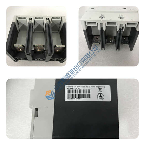
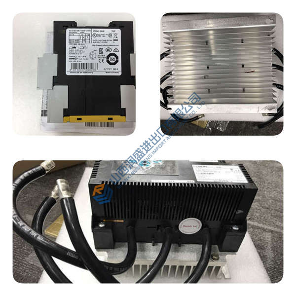
Applied Materials,Inc.is one of the world’s largest manufacturers of semiconductors and display equipment.The company was founded in 1967 and is headquartered in Santa Clara,California.Applied Materials provides innovative equipment,services and software solutions for the semiconductor,display and other high-tech industries.
Product description
Applied Materials’product line is very broad,including the following areas:
Semiconductor equipment:
Etching equipment:used to remove material during semiconductor manufacturing to form the desired circuit pattern.
Deposition equipment:used to deposit various thin film materials on semiconductor wafers,such as metals,oxides,nitrides,etc.
Ion implantation device:Used to inject specific ions into semiconductor wafers to change their electrical properties.
Chemical Mechanical polishing(CMP)equipment:for flattening the surface of semiconductor wafers.
Metering and inspection equipment:used to measure and inspect various parameters of semiconductor wafers to ensure product quality.
Display equipment:
Thin-film transistor(TFT)equipment:used to manufacture thin-film transistors in liquid crystal displays(LCDS)and organic light-emitting diode(OLED)displays.
Vacuum equipment:Used to provide a vacuum environment during display manufacturing.
Other products and services:
Application Global Services(AGS):Provides equipment maintenance,repair,upgrade and optimization services.
Software Solutions:Provides software tools for semiconductor and display manufacturing processes to improve production efficiency and yield.
Product parameter
Due to the wide variety of Applied Materials products,the parameters of each product are different.In general,the parameters of the product include:
Size and weight:The physical size and weight of the device.
Power requirement:The power required by the device.
Processing capacity:The number of wafers or substrates that a device can process per hour or per day.
Accuracy and uniformity:The accuracy and uniformity of the equipment during processing.
Reliability:The average trouble-free uptime of a device.

Product application
Applied Materials’products are widely used in the following areas:
Semiconductor manufacturing:Used to manufacture various types of semiconductor chips,such as microprocessors,memory,logic circuits,etc.
Display manufacturing:Used to manufacture liquid crystal display(LCD),organic light emitting diode(OLED)display.
Other high-tech industries:such as solar cells,light-emitting diodes(LED)and so on.
Brand introduction
Applied Materials is one of the leaders in the semiconductor and display device industry with strong brand awareness and market share.The company is known for its technological innovation,excellent product quality and excellent customer service.The Applied Materials logo is a blue”AMAT”,simple and modern.
Sum up
Applied Materials is a leading global manufacturer of semiconductors and display devices,offering a broad range of products and services to meet the needs of customers in the semiconductor,display and other high-tech industries.The company is known for its technological innovation,excellent product quality and excellent customer service and is one of the leaders in the industry.


