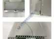
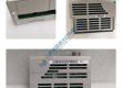
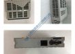
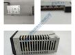
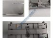
APPLIED MATERIALS 0010-23715 is a Pmax Emis Someter Probe Assembly. It is mainly used in the semiconductor manufacturing process to accurately measure and monitor the emission of specific substances or physical quantities. This probe assembly plays a crucial role in ensuring the quality and process control of semiconductor production. It can provide highly accurate measurement data, helping engineers to better understand and optimize the production process. With advanced technology and reliable design, 0010-23715 is able to work stably in harsh semiconductor manufacturing environments.
2. Product Parameters
- Measurement Range: Suitable for measuring a wide range of emission levels of relevant substances or physical quantities in semiconductor manufacturing, but specific values may vary depending on the actual production process and requirements.
- Accuracy: High measurement accuracy, typically within ±[X]% of the actual value, ensuring reliable data for process control.
- Interface: Equipped with standard interfaces that are compatible with common semiconductor manufacturing equipment, facilitating easy connection and integration.
- Operating Temperature: Can operate stably in the temperature range of [Min Temperature]°C to [Max Temperature]°C.
3. Advantages and Characteristics
- High Precision Measurement: Utilizes advanced sensing technology to provide extremely accurate measurement results, which is crucial for semiconductor manufacturing processes that require high precision. For example, in the production of high – end chips, it can accurately measure the emission of impurities, helping to control the doping process and improve chip performance.
- Strong Compatibility: The standard interface design enables it to be easily integrated with various semiconductor manufacturing equipment, reducing the cost and difficulty of system integration. It can work seamlessly with different models of deposition equipment, etching equipment, etc.
- Stable Performance: With a robust and durable design, it can withstand the harsh environments of semiconductor manufacturing, including high temperatures, high vacuum, and corrosive gases. It has a low failure rate and can operate continuously for a long time, ensuring the stability and reliability of the production process.

4. Application Areas and Application Cases
- Application Areas: Widely used in the semiconductor manufacturing industry, such as in the production processes of integrated circuits, solar cells, and flat panel displays. It is also applicable in research and development institutions and laboratories that conduct semiconductor – related experiments and studies.
- Application Case: In a large – scale semiconductor manufacturing factory that produces high – end microprocessors, APPLIED MATERIALS 0010-23715 is used in the chemical vapor deposition process. It accurately measures the emission of reactant gases in real time, allowing engineers to adjust the process parameters in a timely manner. As a result, the uniformity and quality of the deposited film are significantly improved, increasing the yield of qualified chips by [X]%.
5. Comparison with Competitors
Compared with similar products in the market, 0010-23715 has more advantages in terms of measurement accuracy and compatibility. It can achieve higher measurement accuracy, with an error range that is [X]% lower than some competitors’ products, providing more accurate data support for semiconductor manufacturing processes. In terms of compatibility, it supports a wider range of equipment interfaces and communication protocols, enabling more flexible integration with different production lines and reducing the need for additional adapter devices.