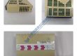
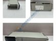
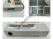
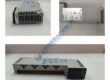
Based on the available information, the AMAT 0010-02342 is identified as a Heater Assembly, likely used in Applied Materials (AMAT) semiconductor manufacturing equipment. Given the numerical proximity to the previous model, it’s probable this component is also associated with the Centura platform or another similar AMAT system.
Product Introduction
The AMAT 0010-02342 Heater Assembly is a crucial component within the thermal management system of Applied Materials’ advanced semiconductor manufacturing equipment. This AMAT 0010-02342 is designed to provide precise and uniform heating within the process chamber, a critical factor for achieving the desired thin film deposition or etching characteristics on silicon wafers. Manufactured by Applied Materials, a global leader in semiconductor equipment innovation, the AMAT 0010-02342 underscores the company’s commitment to delivering high-performance and reliable solutions for the fabrication of integrated circuits. The technical positioning of this Heater Assembly highlights its importance in ensuring process uniformity, repeatability, and ultimately, the quality of the semiconductor devices produced. As an integral part of the automation and control architecture of AMAT process chambers, the AMAT 0010-02342 contributes significantly to the overall efficiency and yield of semiconductor manufacturing by maintaining the precise thermal environment required for various processing steps.
Core Advantages and Technical Highlights
The AMAT 0010-02342 Heater Assembly offers several key advantages vital for the demanding thermal control requirements of semiconductor manufacturing:
Precise Temperature Control: The 0010-02342 is engineered to deliver highly accurate and stable temperature control within the process chamber. This precision is essential for ensuring uniformity and repeatability of thin film deposition or etching processes across the wafer surface.
Uniform Heating: The design of the AMAT 0010-02342 prioritizes uniform heat distribution within the processing zone. This uniformity is critical for achieving consistent material properties and device performance across the entire wafer.
High Reliability: Built by Applied Materials to meet the stringent standards of the semiconductor industry, the AMAT 0010-02342 is designed for high reliability and longevity. This minimizes equipment downtime and ensures consistent process performance over extended periods.
Vacuum Compatibility: The materials and construction of the AMAT 0010-02342 are specifically chosen to be compatible with the high-vacuum environments prevalent in semiconductor processing chambers, preventing outgassing and contamination.
Integrated Temperature Sensing: Typically equipped with an integrated temperature sensor, such as a thermocouple, the AMAT 0010-02342 provides real-time temperature feedback to the process control system. This closed-loop control enables precise and dynamic temperature adjustments.
Optimized Thermal Efficiency: The design of the 0010-02342 likely incorporates features to maximize thermal efficiency, ensuring that the required process temperatures are achieved and maintained with minimal energy consumption.

Typical Application Scenarios
The AMAT 0010-02342 Heater Assembly is a fundamental component in various thin film deposition and etching processes within Applied Materials’ semiconductor manufacturing equipment, particularly likely within the Centura platform. In Chemical Vapor Deposition (CVD) processes, the AMAT 0010-02342 provides the necessary thermal energy to drive the chemical reactions that form thin films on the wafer surface. Similarly, in Physical Vapor Deposition (PVD) processes like sputtering, precise heating can be required for substrate preparation and to influence film properties. In plasma etching processes, the AMAT 0010-02342 helps to control the wafer temperature, which is a critical parameter affecting the etch rate, selectivity, and profile. Across these diverse applications, the AMAT 0010-02342 ensures the uniform and stable thermal environment required to achieve the desired film characteristics and device performance. Its reliability and precise control are essential for maximizing wafer yield and maintaining the high standards of quality in semiconductor manufacturing.