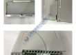
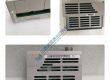
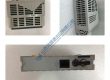
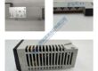
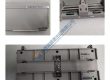
Description: The 0021-16781 AMAT is identified as a SHIELD, UPPER, 300MM, REV 2.0 SIP CU from Applied Materials (AMAT). This is a crucial component within AMAT’s Physical Vapor Deposition (PVD) systems, specifically designed for 300mm wafer processing utilizing SIP (Single In-situ Plasma) Copper technology. This upper shield plays a vital role in protecting specific areas of the process chamber and ensuring precise copper deposition on the 300mm silicon wafers.
Application Scenarios: Consider a high-volume semiconductor manufacturing facility producing advanced integrated circuits with copper interconnects on 300mm wafers. During the PVD process for copper deposition in an AMAT SIP chamber, it’s essential to prevent unwanted deposition on critical areas of the chamber and to help shape the deposition flux for optimal uniformity on the wafer. The 0021-16781 AMAT Upper Shield is strategically positioned above the wafer to perform this function. By accurately shielding certain regions, it ensures that the copper film is deposited only where intended, contributing to the precise fabrication of the intricate wiring within the microchips. The proper functioning of this upper shield is paramount for achieving high-quality copper interconnects and maximizing yield in advanced semiconductor manufacturing.
Parameter
| Main Parameters | Value/Description |
|---|---|
| Product Model | 0021-16781 |
| Manufacturer | Applied Materials (AMAT) |
| Product Category | Shield, Upper |
| Application | 300mm Wafer PVD (Physical Vapor Deposition), SIP Copper Technology |
| Wafer Size Compatibility | 300mm |
| Revision | Rev 2.0 |
| Material | Copper (Cu) (Based on “SIP CU” designation) |
| Condition | New or Used (commonly found on the market) |
| Associated Terms | Process Kit Part, Chamber Shield |
| Function | Protects chamber areas and shapes deposition flux |
| Mounting | Located in the upper section of the PVD chamber |

Technical Principles and Innovative Values:
- Innovation Point 1: Optimized for SIP Copper PVD: The 0021-16781 AMAT is specifically designed for AMAT’s Single In-situ Plasma (SIP) copper deposition process on 300mm wafers, ensuring compatibility and optimal performance within these advanced metallization steps.
- Innovation Point 2: Upper Chamber Protection: As an “upper shield,” this component protects the upper regions of the PVD chamber from copper deposition, minimizing maintenance requirements and preventing particle contamination that could affect wafer quality.
- Innovation Point 3: Deposition Flux Shaping: The precise geometry of the upper shield helps to shape the plasma and the flux of copper atoms towards the wafer, contributing to improved film uniformity across the large 300mm surface.
- Innovation Point 4: Material Compatibility: The use of copper (Cu) in its construction ensures compatibility with the copper sputtering process and helps to minimize the introduction of foreign materials into the deposition environment.
Application Cases and Industry Value: In a leading-edge semiconductor foundry manufacturing high-performance logic devices with copper interconnects on 300mm wafers, achieving uniform and controlled copper deposition is critical for device performance and reliability. The Applied Materials 0021-16781 Upper Shield plays a crucial role in the PVD process by preventing unwanted copper deposition on the chamber walls and by helping to create a uniform flux of copper ions towards the wafer. This leads to more consistent film thickness and electrical properties across the wafer, resulting in higher yields and improved performance of the final integrated circuits.
Related Product Combination Solutions:
- Applied Materials PVD Chamber Assembly (SIP Copper): The complete PVD chamber that houses the 0021-16781 upper shield, along with the sputtering target, wafer pedestal, and other shielding components.
- Applied Materials Lower Shields/Clamps: Components located below the wafer that work in conjunction with the upper shield to define the deposition area and protect other chamber regions.
- Applied Materials Process Control Software: The software that manages the overall PVD process, including the plasma parameters and deposition times that rely on the proper function of the upper shield.
- DC Power Supplies: Provide the power to the sputtering target, generating the copper plasma that is directed towards the wafer with the help of the upper shield.
- Argon Gas Delivery System: Argon is typically used as the sputtering gas in copper PVD, and its flow and pressure are critical parameters for the deposition process influenced by the chamber geometry including the upper shield.
- Brooks Automation Wafer Handling Robots: Precisely load and unload 300mm wafers into the PVD chamber, ensuring proper positioning relative to the upper shield and the sputtering target.
- Thin Film Metrology Tools: Used to measure the thickness, uniformity, and electrical properties of the deposited copper films, providing feedback on the effectiveness of the upper shield and the overall PVD process.
- Vacuum Systems for PVD Chambers: Maintain the ultra-high vacuum environment necessary for high-quality PVD processes, with the shields helping to contain the deposition within a defined area.
Installation, Maintenance, and Full-Cycle Support: The 0021-16781 AMAT Upper Shield requires careful installation within the Applied Materials PVD chamber, typically performed by trained AMAT service engineers to ensure proper alignment and sealing. Routine maintenance may involve periodic inspections for any signs of copper buildup, erosion, or damage. Cleaning or replacement of the shield according to AMAT’s maintenance schedules is important to maintain optimal deposition uniformity and prevent particle contamination.
Applied Materials provides comprehensive technical support for their PVD equipment, including components like the 0021-16781 upper shield. This includes detailed chamber assembly diagrams, maintenance procedures, and access to their global network of service engineers for on-site assistance and genuine AMAT spare parts. AMAT’s commitment to full lifecycle support aims to ensure that users can maintain the optimal performance and yield of their advanced semiconductor manufacturing equipment.